LCD Pin Assignments
|
Pin number |
Symbol |
Level |
I/O |
Function |
|---|---|---|---|---|
|
1 |
Vss |
- |
- |
Power supply (GND) |
|
2 |
Vcc |
- |
- |
Power supply (+5V) |
|
3 |
Vee |
- |
- |
Contrast adjust |
|
4 |
RS |
0/1 |
I |
0 = Instruction input |
|
5 |
R/W |
0/1 |
I |
0 = Write to LCD module |
|
6 |
E |
1, 1->0 |
I |
Enable signal |
|
7 |
DB0 |
0/1 |
I/O |
Data bus line 0 (LSB) |
|
8 |
DB1 |
0/1 |
I/O |
Data bus line 1 |
|
9 |
DB2 |
0/1 |
I/O |
Data bus line 2 |
|
10 |
DB3 |
0/1 |
I/O |
Data bus line 3 |
|
11 |
DB4 |
0/1 |
I/O |
Data bus line 4 |
|
12 |
DB5 |
0/1 |
I/O |
Data bus line 5 |
|
13 |
DB6 |
0/1 |
I/O |
Data bus line 6 |
|
14 |
DB7 |
0/1 |
I/O |
Data bus line 7 (MSB) |
LCD Instructions
|
Instruction |
Code |
Description |
Execution time** |
|||||||||
|---|---|---|---|---|---|---|---|---|---|---|---|---|
|
RS |
R/W |
DB7 |
DB6 |
DB5 |
DB4 |
DB3 |
DB2 |
DB1 |
DB0 |
|||
|
Clear display |
0 |
0 |
0 |
0 |
0 |
0 |
0 |
0 |
0 |
1 |
Clears display and returns cursor to the home position (address 0). |
1.64mS |
|
Cursor home |
0 |
0 |
0 |
0 |
0 |
0 |
0 |
0 |
1 |
* |
Returns cursor to home position (address 0). Also returns display being shifted to the original position. DDRAM contents remains unchanged. |
1.64mS |
|
Entry mode set |
0 |
0 |
0 |
0 |
0 |
0 |
0 |
1 |
I/D |
S |
Sets cursor move direction (I/D), specifies to shift the display (S). These operations are performed during data read/write. |
40uS |
|
Display On/Off control |
0 |
0 |
0 |
0 |
0 |
0 |
1 |
D |
C |
B |
Sets On/Off of all display (D), cursor On/Off (C) and blink of cursor position character (B). |
40uS |
|
Cursor/display shift |
0 |
0 |
0 |
0 |
0 |
1 |
S/C |
R/L |
* |
* |
Sets cursor-move or display-shift (S/C), shift direction (R/L). DDRAM contents remains unchanged. |
40uS |
|
Function set |
0 |
0 |
0 |
0 |
1 |
DL |
N |
F |
* |
* |
Sets interface data length (DL), number of display line (N) and character font(F). |
40uS |
|
Set CGRAM address |
0 |
0 |
0 |
1 |
CGRAM address |
Sets the CGRAM address. CGRAM data is sent and received after this setting. |
40uS |
|||||
|
Set DDRAM address |
0 |
0 |
1 |
DDRAM address |
Sets the DDRAM address. DDRAM data is sent and received after this setting. |
40uS |
||||||
|
Read busy-flag and address counter |
0 |
1 |
BF |
CGRAM / DDRAM address |
Reads Busy-flag (BF) indicating internal operation is being performed and reads CGRAM or DDRAM address counter contents (depending on previous instruction). |
0uS |
||||||
|
Write to CGRAM or DDRAM |
1 |
0 |
write data |
Writes data to CGRAM or DDRAM. |
40uS |
|||||||
|
Read from CGRAM or DDRAM |
1 |
1 |
read data |
Reads data from CGRAM or DDRAM. |
40uS |
|||||||
Remarks:
- DDRAM = Display Data RAM.
- CGRAM = Character Generator RAM.
- DDRAM address corresponds to cursor position.
- * = Don't care.
- ** = Based on Fosc = 250KHz.
LCD Bit Names
|
Bit name |
Settings |
|
|---|---|---|
|
I/D |
0 = Decrement cursor position |
1 = Increment cursor position |
|
S |
0 = No display shift |
1 = Display shift |
|
D |
0 = Display off |
1 = Display on |
|
C |
0 = Cursor off |
1 = Cursor on |
|
B |
0 = Cursor blink off |
1 = Cursor blink on |
|
S/C |
0 = Move cursor |
1 = Shift display |
|
R/L |
0 = Shift left |
1 = Shift right |
|
DL |
0 = 4-bit interface |
1 = 8-bit interface |
|
N |
0 = 1/8 or 1/11 Duty (1 line) |
1 = 1/16 Duty (2 lines) |
|
F |
0 = 5x7 dots |
1 = 5x10 dots |
|
BF |
0 = Can accept instruction |
1 = Internal operation in progress |
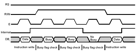
LCD 8 Wire Interface Timings
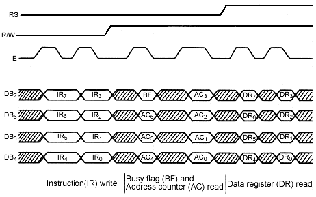
LCD 4 Wire Interface Timings
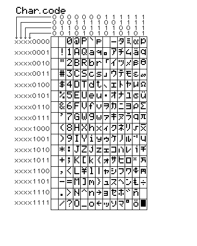
LCD Character Set
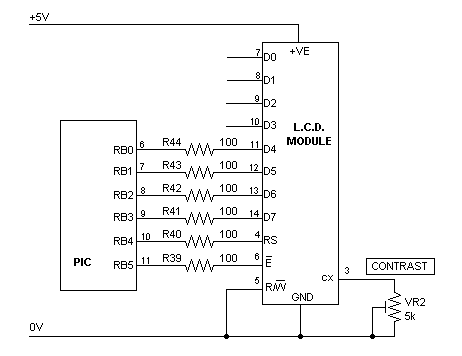
LCD Circuit
Implementation Notes
The LCD panel connected to the PICmicro development board uses four wire mode, which means that you must send the data in two four bit chunks. Note also that the read/write (R/W) line is not connected. Instead it is pulled permanently low, putting the LCD panel into write mode at all times. If you connect this signal you will be able to read from the LCD (note that you would have to put the PICmicro port that you use into input mode to read from the LCD). This can help you get round memory limitations in the PICmicro, since it means that you can use the LCD to hold a copy of the screen information rather than holding it in a variable.